While I have tested some good discrete transistor antilog generator circuit designs, at this time I'm looking into a switching antilog generator. This is an idea from as early as 1957, literally based on just switching transistors. It worked pretty well then, with good performance over temperature for a 100:1 dynamic range using germanium and silicon transistors of the late-50s. As a technical approach, with modern silicon transistors, it is likely to have stronger antilog conformance and much better temperature coefficent performance than a traditional BJT antilog generator. The price paid is that the switching antilog generator works over a smaller total dynamic range: perhaps 7 octaves versus as much as 9 decades for an analog circuit exploiting the inherent antilog current versus Vbe properties of transistors. But the goal here is different: pitch accuracy over a musically useful range matters far more than an enormous dynamic range.
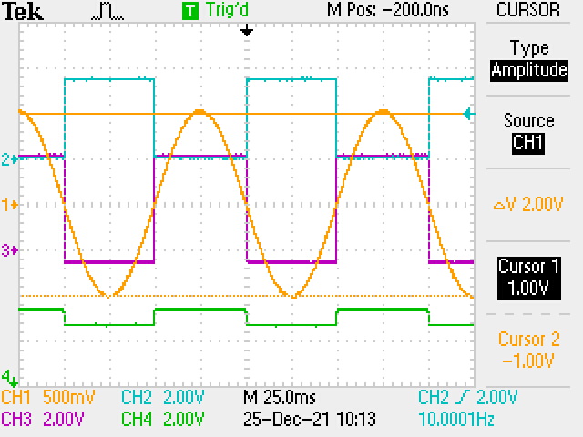
Some 7 octaves (128:1) of real accuracy is actually quite a good range for music, equivalent to an 84-key keyboard for the equal tempered musical scale. A constraint here is obtaining extremely good pitch accuracy over temperature. One example case is multiple simultaneous oscillators that would be used for spectral waveform synthesis.
Some of the component blocks required for a modern higher performance form of the switching antilog circuit include precision comparators and precision summing amplifiers. While I had already created some good discrete voltage comparator circuit designs, they did not offer Vos precision < 1mV, and they tended to to have medium speed of ≈5.0-10μS. It was desirable to have a faster circuit design for perhap 2KHz switching events (antilog pulse waveforms), but with much better DC accuracy than ≈5-10mV in order to align the precision for a 7 octave dynamic range required.
After some research, a circuit design with extreme simplicity emerged. The design in the schematic below is an adaption of "Inexpensive Comparator reacts in 100 nanoseconds," by Richard Becker, a Designer's casebook entry in Electronics, page 70, from September 2, 1968.
Technical notes now follow for this design.
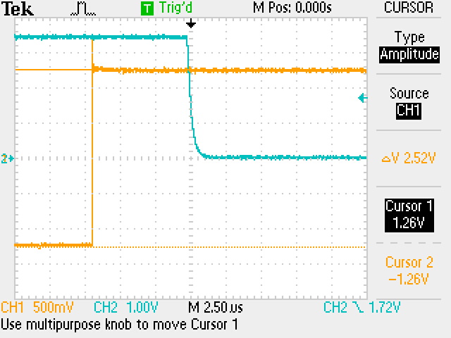
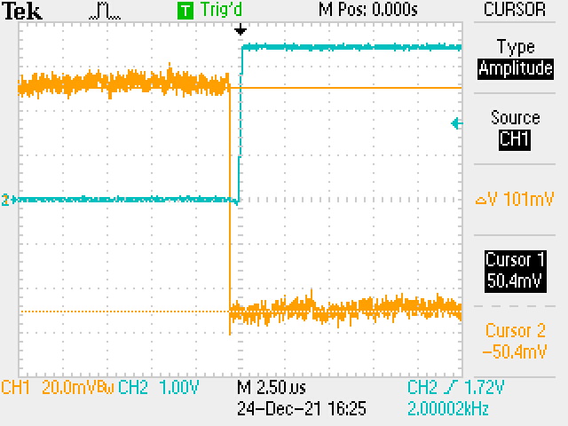
There are some minor differences between the original 1968 circuit and the circuit as implemented in 2021. To provide DC accuracy, the LM394CH monolithic matched dual NPN was used in lieu of a pair of selected matched and thermally-coupled 2N3390 transistors. This "upgrade" is also trimless, and offers much better Vos than most integrated circuit voltage comparators: 30μV. For falling slope inputs that traverse from a positive voltage through 0V to a negative voltage, the propagation delay is < 250 ns. The input voltage range can be quite small, and this transition detected with accuracy around 0V.
The original circuit used +3V for the 2N3904 and 2N3906 output transistors Q3 and Q4, and it had them thermally coupled. For sure, the complementary symmetry as the article suggests is self-balancing. But thermal coupling is not really mandatory for a clean digital output, and the Vcc for these transistors (Q2 and Q3) does not strictly require +3V. The power supply here was ≈3.5V, but the circuit would actually work for any Vcc range from 3V to 5V.
This circuit worked excellently well, comparing my experience with devices like the LM311, LM711, and LM339A. Again, there are some differences between this circuit and the IC comparators. For one, IC comparators accept a larger differential input common mode range, whereas this discrete comparator is only comparing against 0 volts (ground) as an inverting comparator. And due to the circuit design, which uses the ≈3V unipolar output range, the input range is limited to 2.84 Vpp max. Beyond this range a negative input < 1.25V will be compressed by diode clamping in the input transistors; for positive input > 1.25V, the circuit will multitrigger due to phase inversions; and for extremely wide input voltage ranges (e.g. 20Vpp) the power dissipated by the matched dual transistor can become excessive.
But for a 2.5Vpp signal, this comparator beats most IC comparators in both speed and DC accuracy. In particular, I find that the LM339A has a Tpd that is quite often dependent on the rate-of-change of the input signal. For really slow waveforms, the device actually slows down to many microseconds of switching response past threshold. And usually, some hysterisis is required for snap action, but that does not also improve any rate-dependent delay. The 2 mV offset voltage is enormously larger than 30μV.
Used within the aforementioned voltage ranges, the discrete circuit has none of these limitations: it snaps at slow speed signals the same as for faster signals, and it does not require hysterisis. It has the desirable trait of being "constantly" fast for all signal inputs, a boon to performance accuracy in the switching antilog application. Some additional research could suggest circuit design tweaks to enable a larger range of input voltages. With a modest part count, the current design does quite well otherwise.
After the schematic (below), the following scope fotos will annotate the discrete comparator design and its performance.


amplitude response is excellent. what limits our time response? 100ns is only good to 1Mhz
ReplyDeleteSorry for late reply. I'm pretty sure it's the LM394CH dual transistor pair. They are not particularly fast transistors, and are setting the dominant pole here.
Delete