
Schematic of the new DC buffer
This research was to test a new way to use complementary symmetry with the same number of transistors that were used in the Type F1 DC Buffer, which was bundled into the recent New Transistor Circuits post.
What gave rise to this was looking at Sziklai pair as an alternative option to the complementary symmetry current source approach taken with the Type F1 DC Buffer. That idea was aimed at options for higher input impedance and greater bandwidth than the 2-transistor approach taken with the parallel complementary symmetry Type E2 Line Driver.
What a difference a topology makes! With transistors of mostly similar capability, the Sziklai pair clearly yielded some distinct bandwidth and signal drive advantages. This design was much faster and "stiff." A key reason I was looking at such traits was for line driving applications into 600Ω or other low-impedance loads, as well as the ability to drive low-impedance frequency mixers for frequency and waveform synthesis. The Type F1 offered higher input impedance and less bandwidth; the Type F2 offered medium input impedance and much higher bandwidth. Two different performance corners with approximately similar parts counts.
The performance of the new Type F2 design is summarized below, before some indicative scope fotos that show how well this design worked. Next, some notes about components and the circuit design.
The composition of complementary transistors was NPN 2N5088 (Type F2) vs 2N5961 (Type F1) and PNP 2N5087 (both designs). The 2N5088 was introduced in the Type F2 because the application appeared to have Vce ≤ 30V in all cases. It might not have strictly been necessary to use the 2N5961 in the Type F2 design (it supports Vce ≤ 60V), but the lower pair of transistors were right across ±15V rails. That made me nervous, I just don't like circuit designs without good margins.
In any case, both NPN and PNP in both circuits are very high β low-noise transistors, esp. at low collector currents. And the 2N5087 and 2N5088 are a bit more similar. The complementary symmetry pair in the Type F1 do offer excellent temperature stability without any component matching. Similarly, the Type F2 also has excellent temperature stability due to complementary symmetry with a different topology. In both circuit designs, the ΔVbe between NPN and PNP transistors produce a net differential offset voltage that is small and constant, tracking reliably with temperature and the balanced operating conditions.
Both designs utilize a parallel form of emitter follower (e.g. common collector) that drives a parallel 1200Ω ‖ 1200Ω bridge, so as to form a 600Ω equivalent source, looking back into the output. When driving a 600Ω load, this results in precise 2:1 waveform attenuation, which was desired for load matching. The voltage output is of course higher for higher impedance loads. Additionally the resisitive bridge provides very good isolation of the transistors from the load. This is a means to allow long length lines (think of "patch cables") as well as excellent stability under a variety of capacitive loads. For any particular load, the parallel combination of PNP and NPN emitter followers assures very good input-output offset voltage (≤10mV), because the emitter follower on each side of the bridge tends to correct for the inherent Vbe offset of the emitter follower on the other side. This balance is accomplished without transistor matching -- just taking parts out of the parts bag randomly. To get a precision voltage offset to zero, the bridge can be amended (as was done with the Type E2A circuit) by replacing the bridge arms with 1.10kΩ 1% resistors, and taking the output between a 200Ω trimmer. The trimmer allows balancing out residual ΔVbe between NPN and PNP that are otherwise operating at virtually identical conditions, while retaining the effective 600Ω output source impedance.
The big difference that the Sziklai pair makes is that similar to the Darlington pair, the two transistors offer current multiplication. This results in a signal gain of much closer to 1.0x, as versus a single-transistor emitter follower. But the Sziklai only requires a single Vbe drop, instead of two Vbe drops the Darlington does, similar to a conventional single-transistor emitter follower. There are subtle differences in the total amount of current multiplication between the two types of pairs, Sziklai and Darlington, but for audio circuits the Sziklai pair appears to offer better distortion, wider bandwidth, and a bit more power efficiency. In fact, these traits extend into radio frequency applications as well. So, in exchange for the higher input impedance in the Type F1 design, the Sziklai transistor pairs in the Type F2 design drive the parallel 1200Ω ‖ 1200Ω bridge effectively as super transistor NPN + PNP emitter followers.
Here's how it worked out:
- Frequency response DC to 11.0 MHz (-3db) driving 604Ω 1% load.
- Untrimmed input to output DC voltage offset ≤10mV without transistor matching.
- At +4dBm (≈3.48Vpp) output into 604Ω, 3rd harmonic distortion was -51.6 dBc at 440 Hz (A4).
- At +4dBm and 440 Hz, the 5th and 7th harmonic and higher distortion was ≪ -60 dBc.
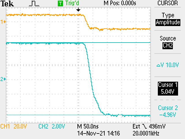
- At 3.48 Vpp into 604Ω the pulse risetime and falltime were balanced, and < 25 ns.
- RP1/RP2 can be chosen to set the bandwidth, while RE1/RE2 set the maximum available current, and can be adjusted for any alternative output drive impedances set by R4/R5.

Usual 1.0 KHz sinusoidal I/O, 20Vpp in, 10Vpp out into ≈600Ω

Triangle wave I/O, same conditions as above

As above, pulse I/O, with traces separated for greater visibility

20 KHz pulse reponse

Rising edge pulse at 10Vpp
Falling edge pulse at 10Vpp

5 MHz pulse response, ≈10Vpp output

5 MHz sinusoidal response

-3dB frequency, ≈11 MHz

+4dBm output

3rd order harmonic at A4 frequency for +4dBm output

5th harmonic is invisible

7th harmonic

Looking at spectral purity, with close in FFT at A4 frequency, 50.0 Hz/div

Triangle wave at 3.48 Vpp into ≈600Ω

Sawtooth wave at 3.48Vpp into ≈600Ω

3.48Vpp A4-frequency pulse into ≈600Ω

3.48Vpp output pulse risetime under load

3.48Vpp output pulse falltime under load
Comments
Post a Comment