This blog post is a bit longer, so it's organized into several sections, which follow below:
- Introduction and Rationales.
- Schematic of the VCA circuit.
- Theory of Operation.
- Trim Procedure.
- Thermal Notes.
- Scope Fotos.
- SDIY Modification Options.
Introduction and Rationales
This project is intended to be a lower-cost, SDIY modifiable version of the Trimless VCA, which did work extremely well. However, the trimless design required 0.1% tolerance resistors, high-precision op amps, and a matched quad transistor integrated circuit. While these components or their replacements are notionally available with enough effort and money, generally their availability is much more limited. This fact makes it harder for others to get components that I had already obtained 20 years ago (like MAT-04 transistor arrays). There is also the greater cost factor. Today, I see increasing component availability problems, as well as longer leadtimes for out-of-stock parts. This is most probably occuring from issues with the current pandamic, with supply chain backups, etc. While this trend is accute now, over many years my "design style" really has transitioned to using commodity industrial parts that have replacement options, and not specialized devices.
I wanted to use the Trimless VCA topology, but with a different surrounding circuit that utilized much more available and also lower-cost components. In particular, the transconductance differential pair should use discrete transistors, and the design general enough to support alternative component choices. This for sure would mean that the design would not be trimless. But at the same time, perhaps the circuit design could be done in such a way that a small number of easy-to-use trims would provide the necessary functionality without deleterious interactions. So, what as required is a simpler yet elegant design like the trimless one, but with only a few trimming stages.
Initially, I started with the LM3900, and unmatched PNP 2N5087 transistors. These transistors invert the current sense compared with the Trimless VCA, so as to be directly compatible with the LM3900 inputs on a +15V supply. I got very far, and built an actual working VCA that used +15V for all of the signal processing. It required a -15V negative power supply voltage only for an output Current Mode Amplifier (CMA) that would allow a normalized bipolar ±voltage swing. This too worked well, except that to use the Norton (or current mode) op amp, numerous voltage levels to offset from ground are required, so as to set up the transconductance differential pair. Other voltage references were required to allow the CMA sub-circuits to work. This takes reference diodes, voltage references, voltage regulators, or similar techniques. But to provide DC accuracy, several trim circuits were required, generally one per voltage reference. I did develop analytic methods to obtain DC precision from this low-cost op amp, and these insights worked -- including an exceptional result of really good CMRR when the LM3900 inputs are fed directly with differential currents. But the component complexity in numbers of resistors plus the number of trimmers was becoming obtrusive, moving away from my original goal of simplicity.
This result led me back to voltage op amps and bipolar power supplies, because this approach yielded simpler circuit designs. The differential pair and current mirror would use unmatched NPN 2N5088 transistors. These are low-noise high-gain devices that have many replacement options. To be clear, this circuit design does not use matched transistors.
I also decided to investigate use of one of the most widely available and low-cost op amps, the LM324. I had used this device for electronic music in the 1970s, and was keenly aware of its limitations. This op amp is an industrial device, it's for sure not an audio device. It has good DC and AC performance, but it is not an outstanding op amp for audio. It is not a NE5532, LM4562, or AD797 audio-grade device. On the other hand it has good gain, good DC offset specs, reasonable frequency response if not pressed for very wide signal swings, a large common mode input range down to the negative supply, and it uses low-power. The single power supply voltage capabilities are not used for this VCA, to simplify interoperability with bipolar input and output signals. The LM324 input bias and operating currents are temperature compensated. The LM324 has a known crossover distortion problem for AC signals. There is a simple mitigation for this problem, which will be discussed below.
A key rationale of this specific effort was to see how much good performance can be obtained from good (but not excellent) low-cost components. And a related concern is simpler circuits in terms of the resulting trimming requirements, and total parts count. And, the idea of this design is to allow potential variant SDIY options and for system longevity with replaceable parts, maintainable circuit boards. As just one example, a LM324A with lower Vos could be substituted, which would provide better differential balance for extremely modest cost change. But other quad op amps could be used instead. And other than the 2N5088 NPN transistors could be used: generally any NPN with high-β at lower collector currents will work well. Some more notes on this and other options are in the SDIY Modification Options section near the end of this blog post.
Before delving into more technical details, some discussion about the role and functionality of the VCA in a synthesizer is in order. A goal of mine is an "all bipolar" sound, meaning that no CMOS or JFET devices should be used in the signal path. So there is a central emphasis is on implementation with circuits using bipolar junction transistors, for the "transistor sound." But another important emphasis is on extremely long service life, robust circuit operation, and removing ESD worries. Relatedly, the synthesizer I am building will not use surface mount technology. I prefer new designs with old replaceable parts over those with new higher-integration analog chip solutions, esp. as these tend to be surface mount devices and sole-sourced. In the Trimless VCA post, I described as well the things I didn't like sonically about VCAs made with CA3080, CA3280, and LM13700 OTAs. Since that post was made, the LM13700N went into lifetime buys and will be obsoleted in May 2022. Anyway, all these concerns are only my view; others may disagree, or may in fact want something different for their synthesizers. All fair: to each their own.
Here are the some observations about what the VCA does in a synthesizer, and how it should (or could) work, a tally of what matters most, and what might not matter at all:
- VCAs should be plentiful: they are how the "voice" of the system gets out. So, a lower cost approach invites more VCAs, and more potential for creative patches. In particular, differential inputs and outputs (like the Moog 902 VCA) seem of great utility for patches, so this VCA design enables that functionality.
- Audiophile VCA performance is totally unnecessary in a synthesizer. For one thing, numerous synthesizer circuits intentionally distort waveforms. So, as long as VCA distortion is not extremely bad, moderate performance is good enough. Similarly, extreme audio bandwidth is a non-concern, because frequencies beyond a certain pitch are not even musically useful. From early FFT testing, the current VCA has mostly 3rd harmonic distortion < -44.4 dBc, at 440 Hz, while other harmonics are far below this. The -3dB bandwidth of this VCA is about 23 kHz. This seems good enough.
- Noise does matter. When the VCA is "off," there should be no discernable audio hiss from the outputs. So, moderate dynamic range is important, but perhaps only 72-80 dB is required. But a 90-100 dB dynamic range is not necessary in a synthesizer context. This VCA provides adequate dynamic range.
- Feedthrough matters, but there is a disparity here too. When the control voltage input is at 0V, the output should be "off," no matter the amplitude of signal inputs. So, signal feedthrough should be extremely small. Control voltage feedthrough however is less of an issue. This VCA design has perhaps ≈50mV control voltage feedthrough with 0V signal input. But this VCA is not intended to enable circuit modification for four-quadrant multiplication, nor for producing large sidebands by using the control voltage input for AM modulation. Tremelo, and dynamic volume control via envelope generators, yes. This VCA provides silence against full signal input when controlled off.
- Support for ±10V (20Vpp) audio signal levels is wasteful and unnecessary. It demands more slew-rate performance from output line drivers, for no benefit. Ultimately, the synthesizer signals go into a mix deck, tape machine, digital recorder, power amplifier, CODEC, etc. A professional +4dBu signal level, or 3.742 Vpp signal is already "loud" for these recording and playback systems. Accordingly, this VCA is designed for ±2.5V nominal levels (5 Vpp), and provides an output sourced from 600Ω. But it can handle ±5V (10Vpp) signals as well. This range of output is such that if 600Ω input impedances are encountered downstream from the VCA outputs, the voltage division of 2 from matching a 600Ω source to a 600Ω load results in signal paths that stay within +4dBu without clipping.

Theory of Operation
Regulated ±15V power enters though a standard PAiA 4-pin 0.1" connector, decoupled with 2.2µF tantalum capacitors rather than electrolytic capacitors, for lower-impedance response at higher frequencies. The ±15V voltages connect to the quad op amp LM324, U1, which is locally decoupled with 0.1µF ceramic capacitors.
To calibrate internal signal levels independent of the power supply voltages, two main voltage references are provided. U2 provides a +2.50V reference and U3 provides a -2.50V reference. The designated LM4040 devices are B-grade, with ±0.2% tolerance. However, it's likely that even lower cost C-grade (±0.5%) or D-grade (±1%) LM4040 devices would also work well, but this was not tested. The 4.99kΩ resistors R1 (for U2) and R16 (for U3) respectively set a quiescent current for the LM4040s from the ±15V supplies that offers low noise and sufficient compliance for current loads that are << 1mA.
The VCA core is a variable transconductance type, comprised of the differential pair Q3/Q4, supplied by the current mirror Q1/Q2. The +2.50 reference U2 provides as baseline for the Q3/Q4 collectors, with balanced current distribution set by R2, P1, and R4/R3 (to Q3/Q4, respectively). This voltage reference also provides an offset voltage to translate a 0-5V control voltage down to -2.5V reference provided by U3 for the current mirror transistors. This is done via R13, tied to the DC op amp for voltage control interface.
U1 op amp 4 (pin 14) translates a 0-5V control voltage down to -2.5V to +2.5V, for voltage compatibility with Q1/Q2 which have their emitters set to -2.5V via voltage reference U3. Current setting resistor R15 sets the input current to the mirror at the Q1 diode-connected transistor from 0 to ≈1mA. Less any β-induced base current losses, the vast majority of this current is reflected about -2.5V from the collector of Q2. The ratio of in/out currents may not be exactly 1:1 due to these losses, but the output current driving the differential pair is always linear in proportion to the input, and it's always monotonic.
The linear VCA action starts to take place when the input control voltage is approximately 500 mV. To allow flexibility in when a 0V control voltage engages volume, an INITIAL VOLUME control is provided via J7 which connects to a 50kΩ front panel potentiometer, as well as to U1 op amp 3 (pin 8), and surrounding circuitry. D1 and R17, plus decouplers C4 and C5 provide an auxilliary -12V reference relative to ground. This reference voltage passes through R18 and then to the 50kΩ front panel potentiometer, forming essentially a 2:1 attenuator at the wiper of the potentiometer. The wiper voltage is buffered by U1 op amp 3 (pin 8), a unity gain buffer. The result is a 0 to -6 volt voltage that goes to the negative summing input of U1 op amp 4, which then inverts that voltage, allowing the front panel INITIAL VOLUME control effectively a 0 to +6V range. This control then can be used to offset the main non-inverting control voltage input (throuh J2 and R9), to set the onset of when the control voltage takes effect. Alternatively, absent any control voltage input at J2, the INITIAL VOLUME can be used as an alternative control voltage generator, allowing 0-5V plus 20% overrange.
The Q3/Q4 differential pair can accept ±2.5 signal inputs at either or both the +INPUT and/or -INPUT. R5/R6 are an attenuator to reduce the input voltage at the +INPUT to approximately ±16.5mV, within the linear range of the differential pair, with considerable additional margin. R7/R8 forms a complementary attenuator for the -INPUT. The current provided by the current mirror though the Q2 collector is split evently between Q3 and Q4 collectors as set by the 100Ω DC BAL adjust trimmer P1. This trimmer allows for correction of inherent ∆Vbe differences as seen on the collectors, between the two unmatched differential transistors when operating at the same current.
Between R2 (49.9Ω), P1, and the 909Ω collector resistors R3/R4, each collector has ≈1kΩ tied to the +2.50 voltage reference U2. When the control voltage at J2 is 0V, the Q3/Q4 collectors sit at a baseline of approximately 2.28V. As the control voltage increases to +5V, the baseline will move down slightly to 2.00V, away from 2.28V. This is a balanced DC common mode signal, the same on each collector. With a ±2.5Vpp signal input at J3, and the full +5V control voltage at CV INPUT J2, an anti-phase AC signal of approximately ±128mV appears at both collectors on top of the DC baseline. If a similar signal were introduced at the -input at J4 instead, the AC signal would be appear at the collectors with the same AC + DC levels, with the phases at the Q3/Q4 collectors reversed when compared to signals from the +INPUT. If both +INPUT and -INPUT were to receive signals, the differential pair would act as a subtractor between the signals.
U1 op amp 2 (pin 7) provides the differential sum of the voltages seen at the Q3/Q4 collectors to the +OUTPUT J5. The op amp rejects the DC common mode signal, amplifying only the AC signal. The collector resistors act effectively as series resistors of ≈1kΩ. They combine with the ≈10kΩ inverting feedback resistor R19, and the non-inverting feedback resistors R20 and trimmer P2, to provide two gain paths. These are inverting and non-inverting, gain paths each of approximately 10x. Thus the peak ground-referenced output of the op amp for the AC signals is 2 * ±128mV * 10 = ±2.56V. While P1 provides a means for nulling the effect of ∆Vbe, the ability of U1 op amp 2 to null a common mode voltage is limited to the CMRR of the op amp plus the gain resistor matching. R20 and P2 provide much better match with the 10.0kΩ R19 than another like 1% tolerance would. This trimmer improves the CMRR, hence DC accuracy of the +OUTPUT J6.
U1 op amp 1 (pin 7) is a unity gain phase inverter, to provide an inverting phase complement to the non-inverting output of op amp 2, out to the -OUTPUT J6. This allows tracking the +OUPUT with inverting phase, within the limits of the Vos of the LM324. To keep this Vos in check better, R25 provides more balance for the resistor combinations to the -input of U1 op amp 1.
All AC signal path op amps in this VCA design feature a 3.3kΩ termination to the -15V rail. These resistors dramatically ameliorate the LM324 crossover distortion effect. I originally used 2kΩ resistors, but the 3.3kΩ worked as well, and this results in less static and dynamic power usage.
Both U1 op amps 2 and 1 have 604Ω output resistors in series to their respective outputs J5/J6 to provide capacitive load isolation as well as a controlled impedence seen looking back into the op amps much lower impedance level. This provides additional short-circuit protection, as a well as a ≈600Ω impedance output.
Trim Procedure
The P1 and P2 trimmers do interact with each other, but in a consistent manner that enables fairly easy trimming. First, the DC BAL trimmer P1 can set the final differential sum at the +OUTPUT up or down about 0V. However, CMMR ADJ trimmer P2 can only set a positive trim about 0V.
One of the inputs (say, the +INPUT) is first given a full scale signal input of ±2.5V. Choose perhaps 1kHz, but the frequency doesn't matter. By examining the DC level seen for CV INPUT = 0V (i.e. silence output), this trim definitely allows 0V output for CV INPUT = 0V.
However, the P1 trimmer can also be set initially to produce a +OUTPUT that is only a few millivolts or so below 0V. Then when the CV INPUT = 5V (i.e. full VCA output), any residual Vos can be seen on an oscilloscope against a 0V mean. Or the Vos can be measured directly by that oscilloscope, if it has digital measurements, like my Tektronix TBS 1064 does. This now larger Vos (it grows with CV) can be trimmed closer to 0 by use of CMRR ADJ P2. Then the +OUTPUT is reset for silent output (CV=0), and the alignment to 0V is checked again.
As neccessary, the produre is repeated. After about 3 repetitions, the alignment allows the +OUTPUT to be center-aligned within 100s of µV of 0V for 0 output, and smaller VCA signal outputs. The final compromise is that the center alignment against 0V with ±2.5 signal outputs is more like <20mV. This is a good compromise in that it preserves the best DC accuracy for lower-level VCA output signals which subsequently might be used for pitch modulation of a VCO.
In keeping with lower cost implementation, both P1 and P2 can be realized with single-turn trimmers and still enable convenient calibration. In fact, an earlier version of design did not have R2, and P2 was originally a 200Ω trimmer. R2 as a 49.9Ω resistors was introduced into the design, and P2 lowered to 100Ω, so as to reduce the range of effect on DC balance. This enabled easier closer to 0 trimming. Multiturn trimming potentiometers could certainly be installed in lieu of single-turn ones in the same PCB footprint -- but these are not really necessary.
Thermal Notes
In the prototype (see foto below), Q1/Q2 and Q3/Q4 were near each other in face-opposing form, but they were not even thermally coupled in any way. Despite this, the VCA offered good performance with testing across multiple days having variable temperatures, albeit in mild California weather. Again, this is not a heat chamber testing regime, but it does show that the VCA design yields good results. In practice, for the module implementation, the pairs of transistors can be bonded together face to face on the PCB, and/or thermally coupled with a heat sink.
The topology of NPN transistors in a current-mirror driving a differential pair, with one ∆Vbe balance trim, and one CMRR trim, combined with negative feedback and good op omp open loop gain of ≈80 dB or more ... all work together yield a thermally stable VCA with good performance.

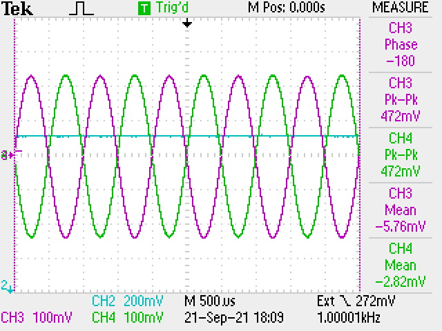
Scope Fotos

Basic I/O with 0-5V control voltage, but signal input over-driven to ±5V

Clean 10 kHz sinusoidal output at full amplitude, with phase delay

15 kHz full-scale sinusoidal output showing some initial Vpp decline and additional phase delay

3.52 kHz triwave I/O (Note: DC level was not calibrated for this foto)

Shape for 3.52 kHz pulse output

10 kHz pulse output at full scale, showing even slopes which reduce TIMD
 Zoom on risetime for 10 kHz pulse output
Zoom on falltime for 10kHz pulse output

Picture-perfect clean differential sawtooth outputs with calibrated DC balance


FFT for 440 Hz sinusoidal output at ≈50mVpp. The 3rd harmonic distortion rises very little as the input voltage rises to ±2.5V.

SDIY Modification Options
The topology of this VCA design allows several options for alternative implementations using the same PCB.
- First, the LM324 could be replaced with a LM324A for slightly better DC accuracy at very modest cost change. However, if anyone doesn't like the bandwidth limitations or any other aspect of the LM324, any pin-compatible quad op amp could be substituted with no other circuit change. So, if a TL074 is more to your liking, and you have them, that device will work, along with others. In the case of a non-LM324/A replacement op amp, the -15V 3.3kΩ termination resistors R14, R21, and R26 do not have to be used.
- At the far end of the extreme of op amp replacement, an expensive OP4227A could be used, improving all aspects of performance. And with replacement of 0.1% resistors for 1% resistors R19, and R20 (plus a wire jumper) the P2 trimmer could be taken out.
- Next, other high-β individual transistors could be used instead of the 2N5088. Generally, these should have β ≈ 100 with Ic = 10µA. The PCB layout is designed to abut TO-92 packages face-to-face with each other, and not an alternative land pattern for parts down like a LM394CH or LS318.
- If you want to match transistors Q3 and Q4 yourself to ∆Vbe < 1mV, P1 could be replaced with a jumper, and R2 replaced with 100Ω 1%, but R3 and R4 should likewise be matched to < 1%, or replaced with 0.1% variants.
- So, hand-matching matching the differential pair transistors Q3/Q4, using higher precision resistors, and using a higher precision op amp, this design could be converted into a trimless form.
- With the circuit design as indicated in the schematic, the LM4040 voltage references can likely be replaced with C or D grade devices, for additional cost savings and/or availability. The absolute voltage difference between U2 and U3 is immaterial for gain control, because the input control voltage already has a variable control to offset where the onset of initial output occurs (e.g. at about 500 mV). Separately, the +2.50 reference U2 appears differentially across the Q3/Q4 collectors, so the absolute value of this voltage is also immaterial. However, it does affect the range of control for R2 and P1, given possibly widely separate ∆Vbe of random pairs of transistors. In the case of the 2N5088, after years of testing, including using these devices in discrete op amps, comparators, and other circuits, the ∆Vbe spread of random pairs tends to be << 10 mV. But other transistor choices could be different.
- A further alternative to using the LM4040 is to replace it with a 2.4 Zener diode like BZX55B2V4, which has a 2% tolerance. Given the potential ≈100mV offset difference between the LM4040 and this Zener diode, some possible tweaking with the value of R2 might be needed. The BZX55 Zener diodes tend to be less noisy than some other Zener diodes that have 1N-registration. If using an alternative Zener diode, some added decoupling might be necessary to reduce noise impingement.
- Different ranges for the INITIAL VOLUME control could be obtained by modifications to the use of D1, R17, and R18. In fact, an additional direct non-inverting electronic input could be made this way without interferring with the existing one. Just omit D1, R17, C4, C5, and C6. R18 could be kept in, if you wanted to isolate the op amp from the direct input; then you wire your extra control voltage input to anywhere along the junction with D1 and R17. Alternatively a direct input could be wired to pin 2 of J7. This option also affords an outboard resistor that could be tied to a front panel jack.

Hello Michael!
ReplyDeleteIf I want to try Quad version of this VCA, will two LM4040 buffered with Op Amp will be sufficient enough to feed all 4 units demands?
Hi DelianDiver! Sorry for such looong response, I just didn't see your comment!
DeleteThe max current draw through the LM4040's about 500μA max. It's set for about 1mA nominal, as that's a modest low-noise corner for this device. If you lowered the 4.99kΩ 1% reference resistor a little bit, perhaps to 3.32kΩ 1%, you'd likely be able to handle all four VCA circuits without adding a buffer op amp.
OTOH, along with your suggestion, if you did buffer the LM4040s with a precision op amp unity gain buffer, then you'd be able to support far more than 4 VCAs.
Happy New Year! Sorry again for the very delayed response.