The following circuit design is an adaption of a 1970s Tektronix instrumentation design. I am calling this design the Type V1, as it's a second generation control-voltage oriented design, after my Type V voltage-adder from early 2000s. I was interested in this design, because for EMS development, there are situations where a full high-performance op amp like the Type X1 DC Amplifier is over-kill, and simple non-inverting gain with offset control is necessary. The amplifier output compliance is from about -0.5V to about +12.4V, and has about 10mA current available. Inputs with a up to -0.5V swing below ground can be accommodated, but the design center is basically an input with a baseline near 0.0V, and up to +10V maximum.
With a modest number of parts, including only 4 transistors, the Type V1 is a small-scale op amp that provides non-inverting gain all in one stage. Plus if offers offset voltage adjustment, for positive voltage input signals. In other words it can be used with a positive-going signal that needs to be precisely adjusted for zero offset at the output, and then potentially range-adjusted for an exact full-scale amplitude limit. The amplfier can take an input control voltage range, and scale it up or down to meet an external interface need. Another application would be normalizing envelope signals. For example, ensuring the output envelope has a 0.0V to +10.0V full-scale range, given an envelope with less amplitude.
In the original application, a sawtooth ramp from 0.0 to about 9.0V is the input, and the RP value was set to 4.02KΩ, which results in gain of about 1.2x. The output was then calibrated to +10V with an 1KΩ attenuating potentiometer (see the schematic).
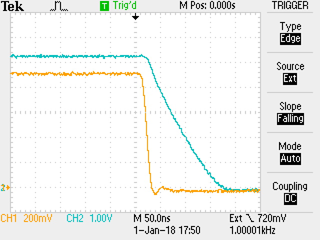
I tested gain configurations from ≈1 to ≈6. At the higher ≈6 gain, the frequency response of the amplifier was flat to beyond 1MHz. In addition, the group delay is very fast, and the amplifier responds well to pulse signals, having very fast propagation delay. At lower gains, the overall AC performance would be even better. So, this amplifier can also be a very clean buffer amplifier for synthesizer module outputs, one that can offer voltage gain from an internal block. This is a nice option when compared with the emitter-follower designs, Type EF and EF2, which can only have a gain ≈1.0x.
On DC performance, there were no deleterious interactions, nor perceptible drift. The circuit is extremely clean, yet very modest. Most of the heavy lifting is done by the differential pair, Q1/Q2, which works well because of the "magic" 2N5088 NPN high-ß transistors. The original circuit used a dual matched-pair transistor, and different transistors otherwise. The 2N5088 allows replacing matched-pairs in most cases, because of extremely good ß. At most operating current ranges, these devices have a minimum ß of 350. So, by differential gain, the open loop Av is approximately 20 • log(350*2), or 56.9 dB. This is not overly large, but is likely to be typically much larger at the operating current supplied by Q3. I don't (yet) have an environmental chamber to run full-sweep temperature steps. But at nominal temperature, the gain is clearly sufficient that no waveform distortion appears visible: e.g. triangle, sawtooth, pulse, and sine waves all appeared very clean on the monitoring scope, over a wide range of frequency. As well, no output DC shift appears, under a variety of signal input types.


With a modest number of parts, including only 4 transistors, the Type V1 is a small-scale op amp that provides non-inverting gain all in one stage. Plus if offers offset voltage adjustment, for positive voltage input signals. In other words it can be used with a positive-going signal that needs to be precisely adjusted for zero offset at the output, and then potentially range-adjusted for an exact full-scale amplitude limit. The amplfier can take an input control voltage range, and scale it up or down to meet an external interface need. Another application would be normalizing envelope signals. For example, ensuring the output envelope has a 0.0V to +10.0V full-scale range, given an envelope with less amplitude.
In the original application, a sawtooth ramp from 0.0 to about 9.0V is the input, and the RP value was set to 4.02KΩ, which results in gain of about 1.2x. The output was then calibrated to +10V with an 1KΩ attenuating potentiometer (see the schematic).
I tested gain configurations from ≈1 to ≈6. At the higher ≈6 gain, the frequency response of the amplifier was flat to beyond 1MHz. In addition, the group delay is very fast, and the amplifier responds well to pulse signals, having very fast propagation delay. At lower gains, the overall AC performance would be even better. So, this amplifier can also be a very clean buffer amplifier for synthesizer module outputs, one that can offer voltage gain from an internal block. This is a nice option when compared with the emitter-follower designs, Type EF and EF2, which can only have a gain ≈1.0x.
On DC performance, there were no deleterious interactions, nor perceptible drift. The circuit is extremely clean, yet very modest. Most of the heavy lifting is done by the differential pair, Q1/Q2, which works well because of the "magic" 2N5088 NPN high-ß transistors. The original circuit used a dual matched-pair transistor, and different transistors otherwise. The 2N5088 allows replacing matched-pairs in most cases, because of extremely good ß. At most operating current ranges, these devices have a minimum ß of 350. So, by differential gain, the open loop Av is approximately 20 • log(350*2), or 56.9 dB. This is not overly large, but is likely to be typically much larger at the operating current supplied by Q3. I don't (yet) have an environmental chamber to run full-sweep temperature steps. But at nominal temperature, the gain is clearly sufficient that no waveform distortion appears visible: e.g. triangle, sawtooth, pulse, and sine waves all appeared very clean on the monitoring scope, over a wide range of frequency. As well, no output DC shift appears, under a variety of signal input types.
Schematic

Work Notes

Scope Fotos
Response to ≈1V step at gain ≈5.76x, 1 KHz PRF


Large signal response at 100 KHz, gain ≈ 5.76x

Large signal frequency response at 1MHz, gain ≈ 5.76x

Comments
Post a Comment