PCB #1 of the Type X1 DC Amplifier Development Board (E1000A) was built with certain soldered down component variations to allow a variety of characterization tests. First, a DC gain configuration of -1 was set with input and feedback precision resistors of 10.0KΩ ±0.05%. Next, the Vos trimming circuit was installed. Then a test load of 604Ω ±1% || 39 pF ±10% was installed. The results of several characterization tests now follow.
0. Test Equipment
Main equipment used was Protek 3040T Power Supply; HP 33120A 10 MHz Function/Arbitrary Waveform Generator; Tektronix TBS1064 60 MHz/1GS/s Four Channel Digital Storage Oscilloscope; Rigol DM3068 6.5 digit DMM.

1. Simple Warm-up Test
After a few minutes of warm-up, the HP 33120A is connected to the input. It generates from 50Ω a 1.00000000 KHz 10 Vpp sinusoidal signal. In observing the input and output together, a very clean inverting sinusoidal output was seen on the Tek TBS1064 monitoring scope.
2. Measure Power Supply Voltages
A spot check of selected variable voltage levels from the Protek 3040T, using the Rigol DM3068. Readings taken only to 5 digits, because power supply noise is seen in the ≈︎100μV range.
Vcc = 15.161V
Vee = -15.184V
The actual values just need to be in the range ±15 V, and are otherwise non-critical to precise functioning of the amplifier.
3. Attempt to Zero Amplifier with Vos Adjustment
With an input jumper to shunt the -input to local ground (the +input also grounded to 200Ω with R13, as part of the Vos adjustment network), the Vos adjustment trimmer R16 was adjusted for as close to zero output as possible, monitored by the DMM. It was easy to trim Vos < 500μV, generally a lot less. After ≈︎2 minutes of measurements, the DMM reported an average of 125μV. This is excellent performance, as the Q1/Q2 differential pair were picked at random, and are not matched pairs! The significance of this find is exemplified with thermals, described next.
4. Thermal Effects Test
It was always known that Q1 and Q2 should be thermally coupled to further reduce offset and drift errors. But this was not initially done in the first build of the E1001A PCB, so as to be able to probe where the limits of the circuit design really are. The thermal test was most revealing. Using a 1000 lumen flashlight to heat up the Q1/Q2 pair, Vos immediately drifted to |±2.5mV|. But each transistor was a separate thermally sensitive component. Shining the light more on one than the other would instantly change the polarity of the Vos. Then, after taking away the light (hence heat) source, something strange happened: a thermal equilibrium established after a few seconds. This state, along with the previously trimmed offset resulted in output voltages < 100 μV! Then, since the two devices are presently isolated, after several thermal time constants, the Vos increased again to it’s original null-trimmed non-equilibrium value, < 500 μV, again averaging much less. So, a key step for effective use of this amplifier will be to mechanically and thermally couple Q1 and Q2. Outstanding DC Vos and drift performance over temperature should result.

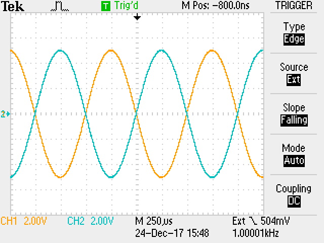
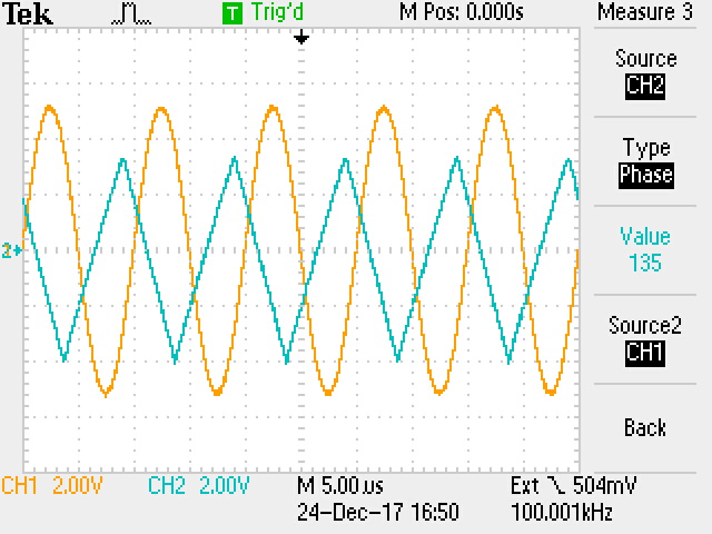
5. Large Signal Phase Response Test
With 10.0 Vpp sinusoidal input, the output matches 179° all the way out to 33 KHz. At 50 KHz, the phase shift is 175°, but the effects of slew-rate limiting are becoming visible. At 100 KHz, a reduced amplitude tri-wave is seen at the output, at 135° phase shift.


6. A 0dBm Small Signal Phase Response Test
With the sinusoidal input reduced to 0dBm, or 2.191 Vpp into 600Ω (0.775 Vrms), the amplifier has inverting output to considerably higher frequencies. The signal and phase relationship is extremely clean at 20 KHz. The output starts changing phase shift from 177º at 100 KHz. At 200 KHz, phase shift is 170º, but slew-rate limiting effects are starting to be seen. At 200 KHz, a definitive triangular shape signal output results, with phase shift at 118º.


7. Small Signal Pulse Dynamics
With 1.000 Vpp square-wave input at 1.00000000 KHz, the amplifier output does have some small damped overshoot pulse aberrations. These aberrations are symmetrical, both rising and falling edges produce the same magnitude of response. Note though that a capacitive load compensation capacitor C8 was not installed on the PCB. By equalizing RC time constant products with the load, it's likely that this small aberration could be flattened considerably.


8. Large Signal Pulse Dynamics
Duplicating the above test with 10.000 Vpp output shows there is almost no visible pulse aberration. So, there is no amplitude dependency in the aberration response. E.g. it's the same size as for the 1.000 Vpp case, but when seen on top of 10x larger output, looks proportionally smaller.


9. Response to Wideband Noise
The HP 33120A can output a wideband noise signal, BW ≈ 10 MHz. With 10.000 Vpp of wideband noise generated into the input, the amplifier clearly passes onto the output only that noise which is within its bandwidth. This is considerably less, as the scope trace below shows.

10. Tone Burst Test
This is a time-domain test which reads on how well the amplifier can respond to burst tones. With a 100 Hz repetition rate, a single cycle of 50.0 KHz sine wave (e.g. a 20μS event) was driven into the amplifier (CH1). The amplifier responds with very fast group delay (CH2): no discernible latency in inverting the input as the output signal, nor are there any deleterious amplitude responses.


0. Test Equipment
Main equipment used was Protek 3040T Power Supply; HP 33120A 10 MHz Function/Arbitrary Waveform Generator; Tektronix TBS1064 60 MHz/1GS/s Four Channel Digital Storage Oscilloscope; Rigol DM3068 6.5 digit DMM.

1. Simple Warm-up Test
After a few minutes of warm-up, the HP 33120A is connected to the input. It generates from 50Ω a 1.00000000 KHz 10 Vpp sinusoidal signal. In observing the input and output together, a very clean inverting sinusoidal output was seen on the Tek TBS1064 monitoring scope.

2. Measure Power Supply Voltages
A spot check of selected variable voltage levels from the Protek 3040T, using the Rigol DM3068. Readings taken only to 5 digits, because power supply noise is seen in the ≈︎100μV range.
Vcc = 15.161V
Vee = -15.184V
The actual values just need to be in the range ±15 V, and are otherwise non-critical to precise functioning of the amplifier.
3. Attempt to Zero Amplifier with Vos Adjustment
With an input jumper to shunt the -input to local ground (the +input also grounded to 200Ω with R13, as part of the Vos adjustment network), the Vos adjustment trimmer R16 was adjusted for as close to zero output as possible, monitored by the DMM. It was easy to trim Vos < 500μV, generally a lot less. After ≈︎2 minutes of measurements, the DMM reported an average of 125μV. This is excellent performance, as the Q1/Q2 differential pair were picked at random, and are not matched pairs! The significance of this find is exemplified with thermals, described next.
4. Thermal Effects Test
It was always known that Q1 and Q2 should be thermally coupled to further reduce offset and drift errors. But this was not initially done in the first build of the E1001A PCB, so as to be able to probe where the limits of the circuit design really are. The thermal test was most revealing. Using a 1000 lumen flashlight to heat up the Q1/Q2 pair, Vos immediately drifted to |±2.5mV|. But each transistor was a separate thermally sensitive component. Shining the light more on one than the other would instantly change the polarity of the Vos. Then, after taking away the light (hence heat) source, something strange happened: a thermal equilibrium established after a few seconds. This state, along with the previously trimmed offset resulted in output voltages < 100 μV! Then, since the two devices are presently isolated, after several thermal time constants, the Vos increased again to it’s original null-trimmed non-equilibrium value, < 500 μV, again averaging much less. So, a key step for effective use of this amplifier will be to mechanically and thermally couple Q1 and Q2. Outstanding DC Vos and drift performance over temperature should result.

5. Large Signal Phase Response Test
With 10.0 Vpp sinusoidal input, the output matches 179° all the way out to 33 KHz. At 50 KHz, the phase shift is 175°, but the effects of slew-rate limiting are becoming visible. At 100 KHz, a reduced amplitude tri-wave is seen at the output, at 135° phase shift.
33 KHz

50 KHz

100 KHz

6. A 0dBm Small Signal Phase Response Test
With the sinusoidal input reduced to 0dBm, or 2.191 Vpp into 600Ω (0.775 Vrms), the amplifier has inverting output to considerably higher frequencies. The signal and phase relationship is extremely clean at 20 KHz. The output starts changing phase shift from 177º at 100 KHz. At 200 KHz, phase shift is 170º, but slew-rate limiting effects are starting to be seen. At 200 KHz, a definitive triangular shape signal output results, with phase shift at 118º.
20 KHz

50 KHz

7. Small Signal Pulse Dynamics
With 1.000 Vpp square-wave input at 1.00000000 KHz, the amplifier output does have some small damped overshoot pulse aberrations. These aberrations are symmetrical, both rising and falling edges produce the same magnitude of response. Note though that a capacitive load compensation capacitor C8 was not installed on the PCB. By equalizing RC time constant products with the load, it's likely that this small aberration could be flattened considerably.
±0.5V Rising Edge Output

±0.5V Falling Edge Output

8. Large Signal Pulse Dynamics
Duplicating the above test with 10.000 Vpp output shows there is almost no visible pulse aberration. So, there is no amplitude dependency in the aberration response. E.g. it's the same size as for the 1.000 Vpp case, but when seen on top of 10x larger output, looks proportionally smaller.
±5.0V Rising Edge Output

±5.0V Falling Edge Output

9. Response to Wideband Noise
The HP 33120A can output a wideband noise signal, BW ≈ 10 MHz. With 10.000 Vpp of wideband noise generated into the input, the amplifier clearly passes onto the output only that noise which is within its bandwidth. This is considerably less, as the scope trace below shows.

10. Tone Burst Test
This is a time-domain test which reads on how well the amplifier can respond to burst tones. With a 100 Hz repetition rate, a single cycle of 50.0 KHz sine wave (e.g. a 20μS event) was driven into the amplifier (CH1). The amplifier responds with very fast group delay (CH2): no discernible latency in inverting the input as the output signal, nor are there any deleterious amplitude responses.
Sine Burst

Tri-wave Burst

Comments
Post a Comment